
Disclaimer: machine translated by DeepL which may contain errors.
The Rigakubu News
The Rigakubu News, May 2025.
Research Student Communicates to Faculty >
Planar Lenses Made Using Only Semiconductor Exposure Processes
Kuniaki Konishi (Associate Professor, Institute for Photon Science and Technology)
While conventional lenses utilize refraction of light,
nanostructures arranged on a plane precisely control the phase of light to
realize a variety of light-collecting characteristics utilizing the properties of light as waves.
meta-lenses have attracted attention in recent years.
The thickness of this structure is about the wavelength of light,
and has the advantage of being extremely thin.
However, the precise fabrication of nanometer-sized structures requires
complicated semiconductor fabrication technology that involves multiple steps.
In this study, we succeeded in developing
a new method that greatly simplifies the
manufacturing process by using photoresist itself, which is used in the semiconductor exposure
process, as a lens material.
![]()
Lenses are basic optical elements used in a wide range of applications such as optical experiments, cameras, and sensors. Conventionally, light has been refracted in an appropriate direction and focused to a single point by grinding transparent material into a spherical shape and making it thicker in the center and thinner toward the periphery. Recently, a new lens called meta-lens, which is different from conventional lenses, has been attracting attention. Meta-lenses realize light focusing by arranging nanostructures of about the wavelength of light on a flat substrate, controlling the phase of transmitted light at each location according to the shape of the nanostructures, and enhancing the light at a single point in the space. Unlike conventional refraction, the meta-lens utilizes the characteristics of light as waves. In addition, meta-lenses have the advantage that the thickness of the nanostructure is about the wavelength of light and can be fabricated very thinly. To realize meta-lenses, semiconductor microfabrication technology that precisely fabricates nanometer-size structures is essential, but with current technology, the gate length of a transistor can be reduced to less than 10 nm, and structures much smaller than the wavelength of visible light (about 350 nm to 750 nm) can be fabricated.
However, the fabrication of meta-lenses requires a complex multi-step process. First, a dielectric or metal thin film is formed on a substrate and a thin layer of photoresist is applied on top of the dielectric or metal thin film. Next, the resist is developed by irradiating it with ultraviolet light using a semiconductor exposure system to form a fine pattern. The patterned resist is then used as a mask for etching, the thin film is processed, and finally the resist is removed. These processes are very complicated, and there has been a need to develop a more efficient manufacturing method.
In this study, we proposed a new method that uses photoresist not only as a mask but also as a lens material itself. The photoresist used is a color resist developed by JSR Corporation, which absorbs specific wavelengths and blocks light. Using this property, a lens called a Fresnel zone plate was easily fabricated. The Fresnel zone plate has a structure of concentrically arranged rings with different widths, and light is focused by the interference of light transmitted between the rings. Unlike conventional processes, the flat lens can be fabricated by a very simple method: a glass substrate is coated with a color resist and irradiated with ultraviolet light using a semiconductor lithography system and then developed.
Using this method, we succeeded in fabricating a large number of Fresnel zone plate lenses on an 8-inch-diameter glass substrate at one time. The width and spacing of the rings became smaller toward the outside, and the outermost ring was about 1 micron. The lenses were used to focus light at a wavelength of 550 nm, and the beam diameter was confirmed to be about 1.1 micron. The same performance was also demonstrated at wavelengths of 450 nm and 650 nm, indicating that this method is suitable for the fabrication of meta-lenses for various wavelengths.
The possibility of mass production of high-performance planar lenses at low cost using existing semiconductor lithography equipment was demonstrated, and this method is expected to open up new possibilities in optical device manufacturing technology.
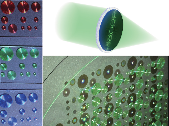 Photographs of planar lenses fabricated using only the semiconductor lithography process and their light focusing
This research result was published in R. Yamada et al. Light: Science & Applications, 14, 43 (2025).
(Press release on January 16, 2025)