
DATE2021.04.15 #Press Releases
Successful enhancement of electrically readable and writable signals in topological antiferromagnets
Disclaimer: machine translated by DeepL which may contain errors.
-A Path to the Development of Nonvolatile Memory Devices Driven at Ultra-High Speeds
Tsai Hanshen (Project Researcher, Institute for Solid State Physics)
Tomoya Higo (Project Associate Professor, Department of Physics / Project Assistant Professor, Institute for Solid State Physics)
Kota Kondo (Senior Researcher, RIKEN)
Shoya Sakamoto (Assistant Professor, Institute for Solid State Physics)
Ayuko Kobayashi (Graduate School of Frontier Sciences, 2nd Year Doctoral Student)
Takumi Matsuo (Graduate School of Frontier Sciences, 1st Year Master's Student)
Masatsugu Miwa (Associate Professor, Institute for Solid State Physics / Associate Professor, Trans-scale Quantum Science Institutes)
Yoshichika Otani (Professor, Institute for Solid State Physics / Professor, Trans-scale Quantum Science Institutes / Team Leader, RIKEN)
Satoru Nakatsuji (Professor, Department of Physics / Project Professor, Institute for Solid State Physics / Director, Trans-scale Quantum Science Collaborative Research Organizations)
Key points of the presentation
- In devices using antiferromagnet Mn3Sn, electrically read/write signals have been enhanced by a factor of three.
- Read signals in the millivolt class have been achieved at low currents by successfully controlling the film interface structure.
- This is a major step toward the practical application of nonvolatile memory devices using antiferromagnetic materials, which are expected to operate at ultrahigh speeds.
Announcement Summary
The research group led by Professor Satoru Nakatsuji, Project Associate Professor Tomoya Higo, and Project Researcher Tsai Hanshen of the Institute for Solid State Physics, The University of Tokyo, together with Professor Yoshichika Otani of the Institute for Solid State Physics, RIKEN (concurrently serving as Team Leader of the Center for Emergent Solid State Physics, RIKEN), and Senior Researcher Kota Kondo of the Center for Emergent Solid State Physics, RIKEN, has developed an antiferromagnetic memory device that is expected to be used for practical applications. Research Center for Solid State Physics (RIKEN), Associate Professor Shinji Miwa and Assistant Professor Shoya Sakamoto of the Institute for Solid State Physics, The University of Tokyo, and their research group, in collaboration with a research group led by Senior Researcher Kota Kondo of the RIKEN Center for Emergent Science, and a research group led by Associate Professor Shinji Miwa and Assistant Professor Yoshiya Sakamoto of the Institute for Solid State Physics, The University of Tokyo, have attempted to optimize the film structure of a multilayer thin film device consisting of Mn3Sn, an antiferromagnet (Note 1) that is attracting attention as a key material for next generation information processing devices, and heavy metal The team attempted to optimize the interface structure and succeeded in increasing the electrically readable/writable signal by a factor of three over the previously reported value.
Antiferromagnets have spin (Note 1 ) dynamics two to three orders of magnitude faster than in the THz band and ferromagnets (Note 1), and the smaller interactions between magnetic materials may enable even faster and more highly integrated magnetic devices, including magnetoresistive memory. Mn3Sn is derived from the topological electronic structure It is an antiferromagnet that exhibits a huge response and has been vigorously studied as a promising candidate for magnetic device materials. The method of enhancing electrically readable and writable signals demonstrated in the antiferromagnetic Mn3Sn multilayer thin-film devices is expected to bring a breakthrough in the development of next-generation magnetic devices.
The research results were published online in the international scientific journal Small Science on April 15, 2021.
Publication details
Background of the research
The recent digital transformation of society due to the spread of the Internet has been remarkable, and various technologies have been developed to process enormous amounts of information in a power-saving and high-speed manner. The semiconductor volatile memory used in information processing terminals such as PCs and smartphones and in data center servers requires a large amount of power at all times because the information is lost when the power is turned off. For this reason, alternatives to nonvolatile memory, which can maintain information even when the power is turned off, are being considered.
Magnetoresistive memory using ferromagnetic materials, which can store the direction of magnetization (magnetic poles of a magnet) as "0" and "1" information, is attracting attention as a typical example of nonvolatile memory. Recently, the phenomenon of magnetization reversal using spin current (Note 2) has been discovered as a method of writing magnetization, and is being generalized. In particular, the magnetization reversal phenomenon that occurs when an electric current is applied to a multilayer film consisting of a ferromagnetic material and nonmagnetic heavy metals such as platinum (Pt) and tungsten (W) is called spin-orbit torque magnetization reversal, and is being actively studied as a next-generation technology.
One of the development guidelines for further increasing the speed of magnetoresistive memory is to use antiferromagnetic materials as a substitute for ferromagnetic materials. The reason for this is that antiferromagnetic materials have a spin response speed in the THz band [pico-( 10-12) seconds], which is two to three orders of magnitude faster than ferromagnetic materials. Research and development on information processing using antiferromagnetic materials is being conducted worldwide, and it has already been demonstrated that it is possible to write and read information electrically in the same way as ferromagnetic materials. On the other hand, the small readout signal has been an issue in application.
Research Content and Results
This research group has been studying the antiferromagnet Mn3Sn, which is composed of manganese (Mn) and tin (Sn), and has discovered that responses such as the anomalous Hall effect (Note 3) and the anomalous Nernst effect (Note 4), which have been believed to be difficult to observe in antiferromagnets, appear at room temperature and zero magnetic field. Subsequent studies have shown that the clustered magnetic octupole (Note 5) of the antiferromagnetic spin structure of Mn3Sn (Figure 1a) corresponds to the Weil point (Note 6), which is a topological electronic structure, and the direction of the virtual magnetic field in momentum space (equivalent to 100 to 1000 tesla (T) in real space). It is also clear that the response derived from the Weil point and the virtual magnetic field can be controlled by the orientation of the cluster magnetic octupole. More recently, we have successfully developed a method to electrically control the response using spin-orbit torque, similar to the ferromagnetic magnetoresistive memory described above (Figure 2a-c).
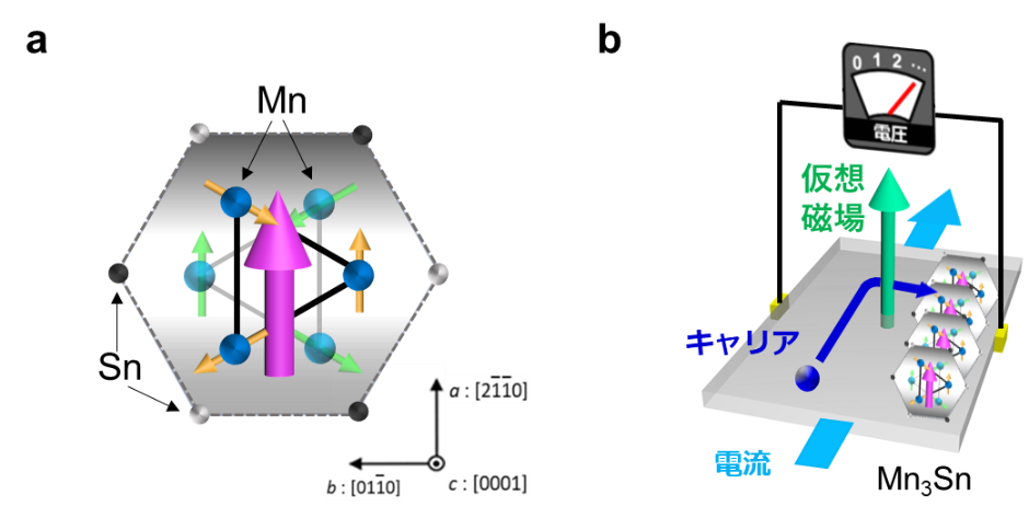
Figure 1: Crystal and magnetic structure of Mn3Sn and overview of the anomalous Hall effect.
(a) The Weyl antiferromagnetMn3Sn has a stacked structure of a Kagome lattice composed of magnetic atoms of manganese Mn (blue spheres) in the c-axis direction. Below 420 K (about 150 °C), the Mn spins exhibit an antiferromagnetic ordering called the inverse 120° structure. Looking at the spins on the two-layer Kagome lattice, we can see that the six spin units, called clustered magnetic octupoles (indicated by the hexagons), are aligned in the same direction. The purple arrows indicate the direction of the magnetic octupoles. (b) In Mn3Sn, due to the effect of a huge virtual magnetic field, an anomalous Hall effect as large as in ferromagnetic materials appears even when the magnetization is very small.
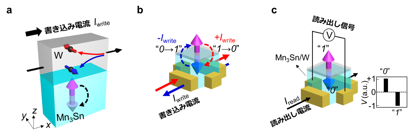
Figure 2: Schematic diagram of magnetic octupole inversion in spin current and the mechanism of information writing and reading in Mn3Sn/nonmagnetic heavy metal (W) devices.
(a) Applying current to theMn3Sn/W device generates a spin current polarized to the red and blue arrows. This spin current causes the antiferromagnetic order of Mn3Sn (magnetic octupole: purple arrow) and the virtual magnetic field to change direction. As a result, the sign of the anomalous Hall voltage reverses. (b) In the Mn3Sn/W device, the direction of the magnetic octupole of the Mn3Sn layer can be controlled by the direction of the write current, and "0" and "1" information can be stored. (c) The information stored by the direction of the magnetic octupole of the above Mn3Sn layer can be read out as a Hall voltage by applying a readout current.
In this study, an element for Hall voltage measurement consisting of a multilayer film containing an antiferromagnetic Mn3Sn polycrystalline film and a heavy metal film was fabricated on a silicon substrate, and the change in Hall voltage due to write current was measured at room temperature. Figure 3a shows the dependence of the Hall voltage on write current at room temperature in the previously reported ruthenium (Ru) /Mn3Sn/W multilayer. Here, a read current of 0.2 mA is added to the Hall voltage measurement in addition to the write current, and a change in Hall voltage of about 25 µV is observed when a write current of about 30 mA is applied. This behavior indicates that the spin current generated in the W layer by applying current to the device inverts the Hall voltage derived from the magnetic octupole of Mn3Sn and the virtual magnetic field (inverted by the spin-orbit torque). In this study, we newly improved the multilayer stacking structure and deposition process, and attempted to enhance the readout signal by changing the crystal orientation of the Mn3Sn layer and the interface structure with the heavy metal. multilayer device with a surface roughness smoothed down to approximately 0.5 nm by removing the Ru layer and improving the heat treatment process after the W layer deposition. In addition, Hall voltage measurements confirmed that electrical control of the readout signal, which is about three times larger than that of the above Ru/Mn3Sn/W multilayer device, is possible (Figure 3b). (Hall voltage) = (readout current) × (Hall resistance). It is known that the Hall voltage increases in proportion to the readout current, but with this device, a voltage of 1 mV can be obtained without heat generation by applying a current of about 3 mA (Figure 3c).
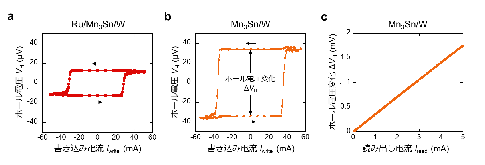
Figure 3: Current dependence of Hall voltage and readout signal enhancement in write and readout experiments and readout signal in Ru/Mn3Sn/W and Mn3Sn/W devices.
(a) Hall voltage dependence of write current at room temperature inRu/Mn3Sn/W devices. (b) Write current dependence of the Hall voltage at room temperature in the Mn3Sn/W device. We confirmed that signals as large as three times larger than those of the above Ru/Mn3Sn/W device can be electrically controlled. A read current of 0.2 mA was added to the Hall voltage measurement in addition to the write current. (c) Readout current dependence of the readout signal (Hall voltage) in the Mn3Sn/W device. 1 mV voltage can be obtained with a readout current of about 3 mA without affecting the temperature rise of the device.
The increase in the readout signal (Hall resistance) is thought to be mainly due to (i) the alignment of the crystal grains of the Mn3Sn layer in the direction of larger readout signal and (ii) the smoothing of the interface between Mn3Sn and W due to the improved deposition process. This device has the characteristic that the current required for writing is lowered by reducing the device size, resulting in a larger readout signal.
Future Prospects
In recent years, development of methods for writing and reading information using antiferromagnetic materials has been vigorously pursued. In this research, information is written to the antiferromagnet Mn3Sn using spin-orbit torque. Therefore, the same device structure as in the ferromagnetic case can be used, and the technology currently used in nonvolatile magnetoresistive memory can be applied. The "readout signal enhancement method in thin-film devices consisting of antiferromagnetic Mn3Sn and heavy metals" demonstrated in this study provides useful knowledge for the development of magnetic devices that can be driven at ultrahigh speeds required for high-speed information processing in data centers and BEYOND 5G communications. On the other hand, in order to promote implementation in information devices, it is important to demonstrate ultrafast information processing in picoseconds, which is expected in antiferromagnetic materials, and to further enhance the readout signal. In addition, properties originating from the topology of materials have attracted much attention in recent years in solid state physics, and the electrical control of the Weil particle itself is also of great academic interest. The method we have developed to electrically control Weil particles and efficiently obtain readout signals is expected to lead to research on non-equilibrium physics such as dynamics of Weil particles and new phenomena that have not been observed so far.
This research is being conducted as part of the "Development of Functional Magnetic Materials and Devices Based on Topological Electronic Structures" research project under the "Creation of Materials and Devices with Innovative Functions Based on Topological Materials Science" research area (research supervisor: Masahito Ueda) of the Japan Science and Technology Agency (JST) Core Research for Evolutional Science and Technology (CREST). (Research Director: Masahito Ueda), as part of the research project "Development of Functional Magnetic Materials and Devices Based on Topological Materials Science with Innovative Functions" (Research Director: Satoshi Nakatsuji).
Journal
-
Journal name Small Science Title of paper Large Hall Signal due to Electrical Switching of an Antiferromagnetic Weyl Semimetal State Author(s) Hanshen Tsai, Tomoya Higo, Kouta Kondou, Shoya Sakamoto, Ayuko Kobayashi, Takumi Matsuo, Shinji Miwa, Yoshichika Otani, and Satoru Nakatsuji*. DOI Number 10.1002/smsc.202000025 Abstract URL https://onlinelibrary.wiley.com/doi/10.1002/smsc.202000025
Terminology
Note 1: Antiferromagnet, spin, and ferromagnet
A magnetic body is a material that possesses a microscopic magnet due to the spinning motion of electrons, called "spin". These magnetic bodies exhibit magnetic ordering in which macroscopic numbers of spins are aligned in some pattern, and are classified into (1) ferromagnetic bodies in which the spins are aligned in a uniform direction and exhibit large magnetization like a magnet and (2) antiferromagnetic bodies in which neighboring spins are aligned in an antiparallel or mutually canceling manner and the net magnetization is zero or very small. (2) antiferromagnets, in which the net magnetization is zero or very small due to the arrangement of adjacent spins in an antiparallel or canceling manner. ↑up
Note 2 Spin current
In electronics, the flow of charge possessed by electrons, or current, plays an important role. Normally, the spin direction of electrons in the current is random. In spintronics, which actively utilizes the spin degree of freedom of electrons, "spin current," which is the flow of spin, is used. The nonmagnetic heavy metal used in this research generates a spin current in which the spin direction is aligned orthogonally to the current when an electric current is applied. By creating a multilayer film, the spin current generated in the heavy metal layer can be injected into neighboring layers. ↑up
Note 3 Anomalous Hall effect
The phenomenon in which an electromotive force is generated perpendicular to the magnetic field and current in a material capable of conducting electricity is called the Hall effect. This is caused by the direction of motion of electrons flowing as an electric current being bent by the magnetic field when a magnetic field and electric current are applied perpendicular to each other. In ferromagnetic materials with spontaneous magnetization, special antiferromagnetic materials with virtual magnetic fields (an effective magnetic field that exists in wavenumber space, a new physical concept that stems from the topology of the electronic structure), and spin liquids, the Hall effect occurs even when no external magnetic field is applied. This effect is called the anomalous Hall effect. ↑up
Note 4 Anomalous Nernst effect
The Nernst effect is a phenomenon in which an electromotive force is generated in a direction perpendicular to the magnetic field and temperature gradient in a material capable of conducting electricity. This is caused by the bending of the electron flow from the high-temperature side to the low-temperature side due to the magnetic field when the magnetic field and temperature gradient are applied perpendicular to each other. In ferromagnetic materials with spontaneous magnetization or special antiferromagnetic materials with a virtual magnetic field, the Nernst effect appears even in a zero magnetic field, and this is called the anomalous Nernst effect. In this case, an electromotive force can be obtained by directing the magnetization or virtual magnetic field perpendicular to the temperature gradient instead of the magnetic field. Using the anomalous Nernst effect, there is no need to apply an external magnetic field, so power generation and heat flow sensing are possible using only temperature differences, attracting attention from the perspective of energy harvesting. ↑up
Note 5 Cluster magnetic octupole
A magnet has two poles, N and S, but spins arranged at each lattice point of a magnetic material also have two poles, which are also called magnetic dipoles. The characteristic combination of spins created when considering a unit with spins located at multiple lattice points is called a clustered magnetic multipole, and as the number of spins constituting the unit increases to one, two, or three, the names of the combinations change to magnetic dipole, quadrupole, octupole, and so on. In the spin structure of the antiferromagnet Mn3Sn, the unit can be thought of as six spins arranged on two Kagome lattices and having a clustered magnetic octupole as shown in Figure 1b. This clustered multipole acts as a parameter that controls the Weil point and the direction of the virtual magnetic field in Mn3Sn, for example, and even in combinations where the sum of the magnetizations is zero, it shows a giant response, as seen in ferromagnets. ↑up
Note 6 Weil point
Substances with particles of zero mass (Weil particles) described according to the Weil equation proposed by Hermann Weil in 1921 are called Weil half-metals. Since neutrinos were found to have tiny masses in the Super-Kamiokande experiment, the Weil particle was thought to be an illusory particle that does not exist in nature. In the Weil semimetals, the Weil points appear as pairs with different chirality (right-handed and left-handed degrees of freedom) as a topological electronic structure. This pair of Weil points corresponds to the N and S poles of a magnet in momentum space. In ordinary Weil semimetals, the Weil points are created by the crystal structure of the material. On the other hand, magnetic materials with Weil points created by magnetism are called Weil magnets (more broadly, topological magnets). In Weil magnets, it is possible to control the Weil points and the associated virtual magnetic field by controlling the magnetic order in an external field such as a magnetic field, which is an attractive property from the viewpoint of application. The virtual magnetic field generated between Weil points is large enough to correspond to an external magnetic field of 100-1000 tesla (T), and is the origin of the giant anomalous Hall effect and other phenomena. ↑up