DATE2024.01.31 #Press Releases
The new hidden properties of quartz crystals are revealed by experiments with heat!
Disclaimer: machine translated by DeepL which may contain errors.
Osaka Metropolitan University
School of Science, The University of Tokyo
Summary of Presentation
Quartz, a familiar mineral since ancient times, is used as an indispensable electronic component in electronic devices such as quartz watches, cellular phones, and gyro-sensors, taking advantage of its electrically vibrating properties. Quartz has a special structure (chiral) that overlaps when mirrored but does not actually overlap, and the effects of having a chiral structure appear in its electrical and thermal properties. Previous research has revealed that when electricity is applied to a chiral metallic material, the magnetic balance of the electrons is disrupted and they are biased either positively or negatively. However, since electricity does not flow in quartz, a chiral nonmetallic material, it has not been clarified what kind of chiral-specific phenomena occur.
A research team led by Kazuki Ohe (then a master's student) and Professor Yoshihiko Togawa of the Osaka Metropolitan University Graduate School of Engineering, Masaki Kato (a doctoral student) and Assistant Professor Hiroyasu Matsuura of School of Science, The University of Tokyo, and their colleagues have succeeded in electrically detecting the rotational motion of atoms as they oscillate along a heat flow applied to a quartz crystal. The team succeeded for the first time in the world in electrically detecting the rotational motion of atoms as they rotate and vibrate along a heat flow applied to a quartz crystal. Since it is possible in principle to "control the flow of heat" and "convert the rotational motion of atoms caused by heating into an electrical signal," this research is expected to contribute to the development of new heat-insulating materials and information processing technology.
The research results were published in "Physical Review Letters" published by the American Physical Society on January 30, 2024.

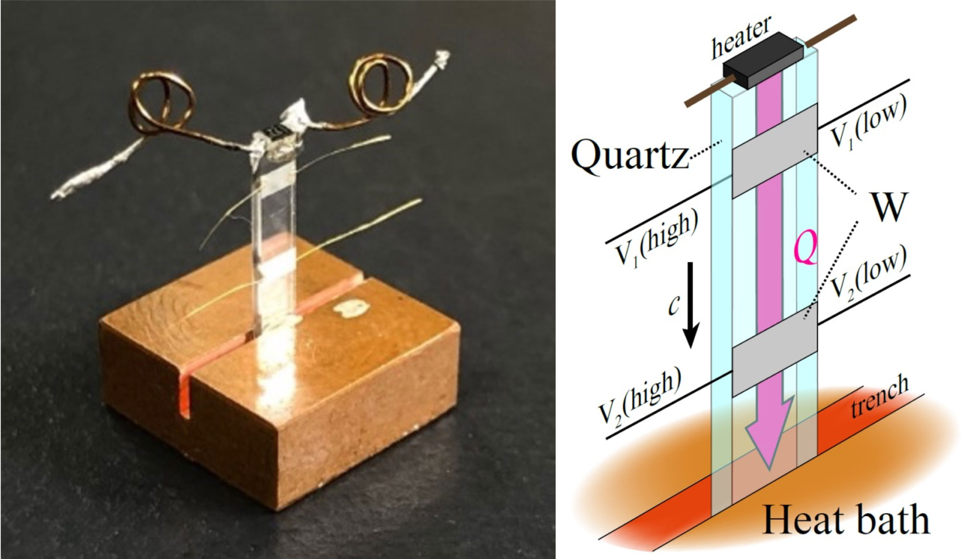
Optical photograph of the crystal device used in the experiment and schematic diagram of the device structure. The size of the copper block is 10 mm square and the crystal is 10 mm x 2 mm x 0.5 mm.
For more information, please visit the Osaka Metropolitan University website.
Journal
-
Journal name Physical Review LettersTitle of paper


