
DATE2021.12.28 #Press Releases
Why is tungsten-doped tin oxide transparent to infrared radiation?
Disclaimer: machine translated by DeepL which may contain errors.
~New Design Guidelines for High Mobility Transparent Electrodes for Next Generation Solar Cells
Yasushi Hirose, Associate Professor, Department of Chemistry
Michitaka Fukumoto (Department of Chemistry, 3rd Year Doctoral Student (at the time of research))
Tetsuya Hasegawa, Professor, Department of Chemistry
Professor, Nagoya Institute of Technology
Koji Kimura, Assistant Professor, Nagoya Institute of Technology
Daiichiro Sekiba (Lecturer, University of Tsukuba)
Key Points of the Presentation
- We have elucidated the mechanism by which a tin oxide transparent electrode (Note 3) to which a trace amount of tungsten (Note 2 ) is added as a donor impurity (Note 1) shows excellent transparent conductivity for visible to near infrared light.
- It has been clarified for the first time that the charge state required for high mobility is stabilized by the hybridization (Note 4 ) of the electron orbital of oxygen in the crystal with tungsten, which has conventionally been treated as a simple negative charge.
- This is expected to lead to the development of new transparent electrodes for next-generation solar cells that can generate electricity even under infrared light.
Summary of the announcement
In recent years, next-generation solar cells that can generate power not only from visible light but also from infrared light have been attracting attention. Transparent electrodes are used to extract power generated by solar cells, but since ordinary transparent electrodes reflect infrared light, materials with high electron mobility (Note 5) are required. Tin oxide thin films doped with trace amounts of tungsten are one such material, but the origin of the high mobility was unknown.
In this study, a research group led by Professor Tetsuya Hasegawa, Associate Professor Yasushi Hirose, and then graduate student Michitaka Fukumoto of The University of Tokyo Graduate School of Science, in collaboration with the Norwegian University of Science and Technology, Nagoya Institute of Technology, University of Tsukuba, and University College London, investigated the structure, electrical conductivity, and electronic state of tungsten-doped tin oxide thin films in detail, It was revealed that tungsten replaces tin atoms in tin oxide crystals as a pentavalent cation, resulting in high electron mobility. Furthermore, using first-principles calculations (Note 6), we have shown that the pentavalent state is stabilized by the hybridization of the d orbital of tungsten and the p orbital of oxygen.
In conventional studies of transparent electrodes, oxygen in crystals has been treated simply as a negative charge, but by considering the hybridization of orbitals with donor impurities based on the results of this research, the development of new transparent electrodes for next-generation solar cells is expected.
Publication details
In recent years, development of high-efficiency solar cells that can generate electricity not only from visible light but also from infrared light has been actively pursued. Transparent electrodes that are transparent to incident light and exhibit high electrical conductivity are used to transfer the power generated by solar cells to external circuits. Indium oxide ( In2O3 ) with tin (Sn) added as a donor impurity and tin oxide ( SnO2 ) with fluorine are widely used as practical transparent electrodes, but these materials have low mobility of conduction electrons and are doped with high concentration of electrons to obtain high electrical conductivity. However, the high concentration of conduction electrons has the property of reflecting infrared rays, resulting in low utilization efficiency of infrared light. Therefore, there is a need for high-mobility transparent electrode materials that provide high electrical conductivity even at low electron concentrations.
Recently, it has been reported that the addition of transition metals as donor impurities to oxide semiconductors such asIn2O3 andSnO2, whose conduction bands consist of metal s-orbitals, can produce high-mobility transparent electrodes. This is believed to be because the d orbitals of the donor impurity do not hybridize with the conduction band of the oxide semiconductor and do not disturb the electronic state. In these materials, the stable charge state changes as the energy of the d-orbital of the donor impurity splits, and it is important to stabilize a state that is +1 valence higher than the metal ion ( In3+ orSn4+) in the base crystal, where the ionization impurity scattering (Note 7), a factor that lowers mobility, is minimized. However, such a charge state is not possible. However, the mechanisms and methods for stabilizing such charge states have not been fully established.
In this study, the research group synthesized a single-crystal thin film of SnO2 with a rutile crystal structure and tungsten (W) as a donor impurity on an aluminum oxide substrate using the pulsed laser deposition method (Note 8 ), and investigated electrical conductivity properties. and an optical transmittance of about 80% for infrared light with a wavelength of 2 μm (Fig. 1).
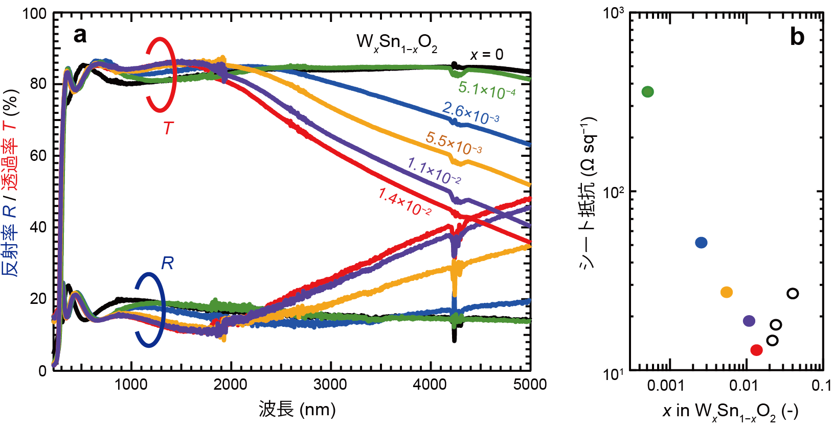
Figure 1: (a) optical transmittance and reflectance and (b) sheet resistance of SnO2 thin films prepared by varying the amount of W addition x. The thin film with x = 0.014 has a sheet resistance of 13.6 Ω sq-1 and transmits over 80% of infrared light up to 2 µm wavelength.
A detailed investigation of the position and charge state of the added W revealed that W displaces Sn as +5 valence ( W5+), which is +1 valence higher than Sn4+ in SnO2, and ionized impurity scattering is suppressed (Figure 2).
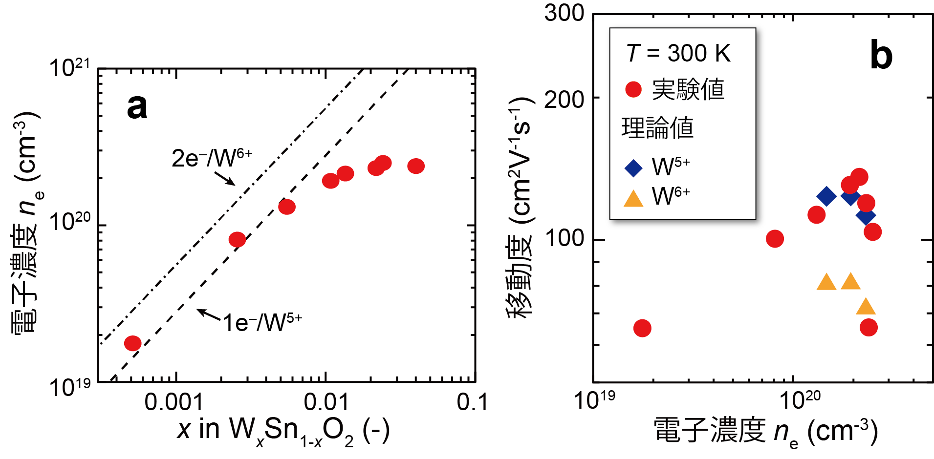
Figure 2: (a) Relationship between W doping level and electron concentration in W-doped SnO2 thin films. At low W concentrations, the values are in good agreement with those assumed for W5+ (dashed line). (b) Electron concentration vs. mobility for W-doped SnO2 thin film. The experimental value (0) is higher than the theoretical upper limit (△) calculated assuming W6+ and is in close agreement with the theoretical upper limit (◇) assuming W5+.
Furthermore, the mechanism by which W, a group 6 element, exists stably in a +5 valence state in SnO2 crystal was investigated using first-principles calculations. The 5d orbital of W splits into (1) a deep level in the band gap and (2) a higher energy level than the lower edge of the conduction band, with the level in (1) becoming a high-spin state with one trapped electron The +5 valence state is stabilized by the emission of one electron from level (2) into the conduction band (Fig. 3a). We also found that the splitting of the 5d orbital of W cannot be explained by the effect of the negative charge of the surrounding oxide ion ( O2-) (crystal field splitting), but is caused by the hybridization with the p orbital of O2- (ligand field splitting) (Fig. 3b).
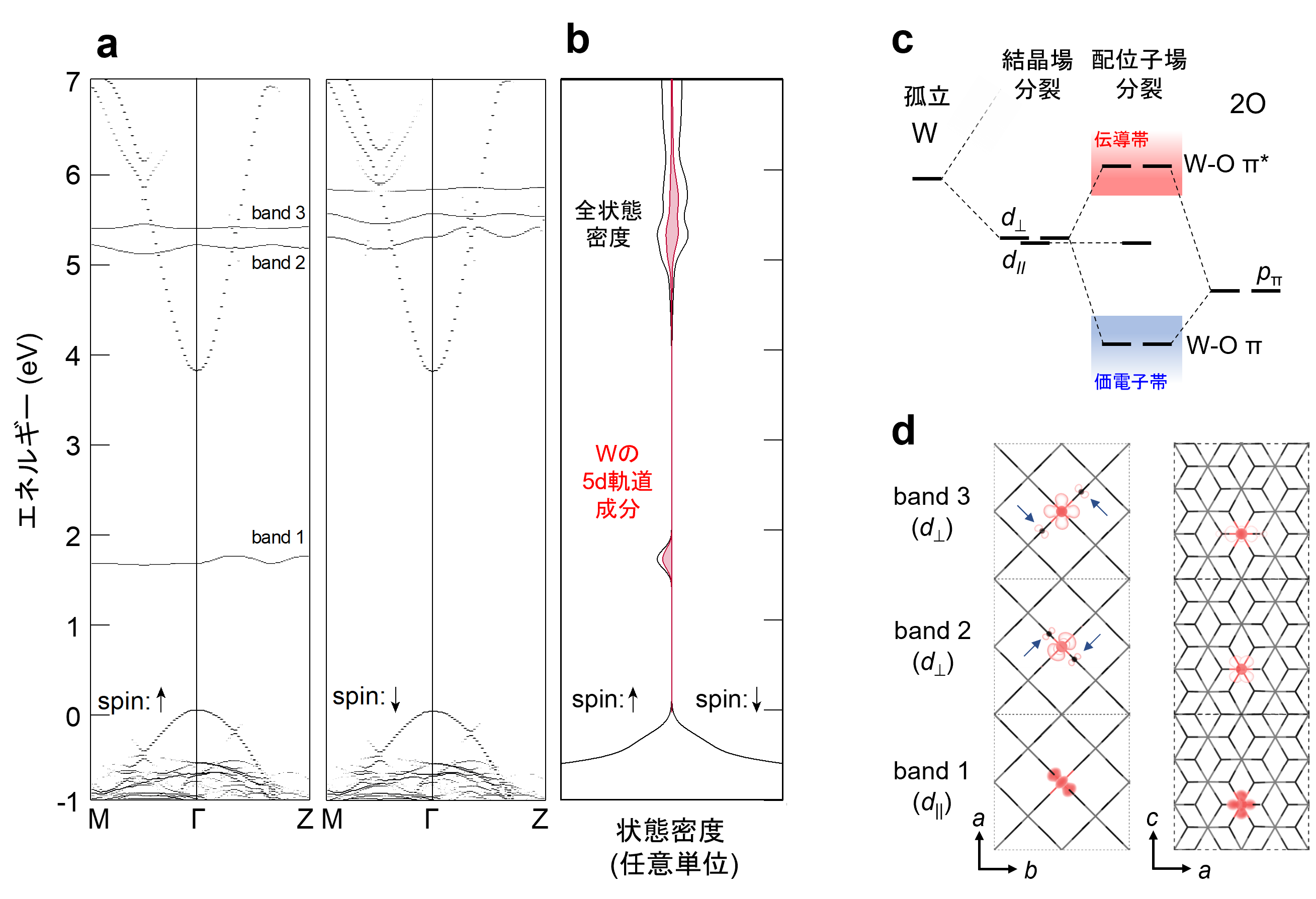
Figure 3: (a,b) (a) band structure and (b) energy distribution of the density of states for W-doped SnO2. W 5+ is stabilized by upward spin electrons (↑) trapped in a high-spin state in band 1 within the band gap. (c) Schematic of d orbital splitting due to hybridization of W 5d and O 2p orbitals. The non-bonding d// forms band 1 in the band gap, while d⊥ is destabilized by antibonding interactions with O 2p orbitals to form bands 2 and 3 in the conduction band. (d) Charge density distribution of band 1-3 projected from the c-axis and b-axis directions; charge densities (arrows in the figure) originating from hybridization with O 2p orbitals can be observed in band 2 and 3 corresponding to d⊥.
It is well known that in transition metal oxides, ligand field splitting has a significant effect on the splitting of the d orbitals of transition metal ions. On the other hand, previous studies of transparent electrodes have only considered the effect of crystal field splitting on the added transition metal compounds. Based on the results of this study, more accurate prediction of the charge state of transition metals in oxide semiconductors and search for new donor impurities will become possible by taking into account the effects of ligand field splitting as well. These findings are expected to contribute to improving the conversion efficiency of next-generation solar cells that use near-infrared light through the development of higher-performance infrared transparent electrodes.
This research was conducted in collaboration with Professor Yoshikazu Hayashi and Assistant Professor Koji Kimura at Nagoya Institute of Technology, Lecturer Daiichiro Sekiba at Tsukuba University, Dr. Benjamin Williamson at Norwegian University of Science and Technology, and Professor David Scanlon of the University College London. This work was supported in part by Grant-in-Aid for Scientific Research on Innovative Areas (A) "Superordered Structural Science" (Area Representative: Yoshikazu Hayashi) and Nanotechnology Platform (JPMXP09A20UT0246, JPMX09A20NM0084) of the Ministry of Education, Culture, Sports, Science and Technology, Japan.
Publication Journals
-
Journal name Advanced Functional MaterialsTitle of Paper Ligand Field-induced Exotic Dopant for Infrared Transparent Electrode: W in Rutile SnO2Author(s) Michitaka Fukumoto, Yasushi Hirose*, Benjamin A. D. Williamson, Shoichiro Nakao, Koji Kimura, Koichi Hayashi, Yuki Sugisawa, Daiichiro Sekiba, David O. Scanlon, and Tetsuya HasegawaDOI Number 10.1002/adfm.202110832Abstract URL
Terminology
Note 1 Donor impurity
An impurity added to a semiconductor to increase the concentration of conduction electrons. ↑up
Note 2 Tungsten
An element with atomic number 74. Because its ionic radius is close to that of tin, it can replace tin in tin oxide crystals. Tungsten-doped tin oxide is widely applied as a gas sensor. ↑up
Note 3 Transparent electrode
An electrode using a transparent conductor, a material that has both high visible light transparency and electrical conductivity. Wide-gap oxide semiconductors doped to degenerate regions are most widely used as transparent conductors. Typical materials are tin-doped indium oxide (ITO) and fluorine-doped tin oxide (FTO). ↑up
Note 4 Hybridization
Hybridization refers to the formation of new orbitals by mixing the electron orbitals of multiple atoms or ions. ↑up
Note 5 Mobility
A value that expresses the ease of movement of electrons and holes in a solid due to an electric field. It is one of the most important values for semiconductor performance. In transparent electrode applications, a higher value improves both conductivity and transparency at the same time. ↑up
Note 6 First-principles calculation
A method to study various physical and chemical properties by numerically calculating the electronic state inside a material from fundamental physical constants without using modeling or empirical parameters. ↑up
Note 7 Ionizing impurity scattering
An effect in which donor impurity atoms added to an oxide semiconductor that have emitted electrons (i.e., become ionized) interfere with electronic conduction. ↑up
Note 8 Pulsed laser deposition method
A method of fabricating thin films by instantaneously evaporating and sublimating materials by irradiating them with a high-intensity pulsed laser pulse and depositing them on a substrate. ↑