
DATE2023.06.14 #Press Releases
Researchers succeed in arranging nanoscale quantum sensors on desired targets
The sensors enable high-resolution magnetic field imaging with applications in superconductors and electronic devices.
June 14, 2023
Overview
1. The University of Tokyo scientists achieve the delicate task of arranging quantum sensors at a nanoscale, allowing them to detect extremely small variations in magnetic fields.
2. The high-resolution quantum sensors will have potential uses in quantum materials and electronic device research. For example, the sensors can help develop hard disks that use nano-magnetic materials as storage elements.
3. This is the world’s first successful high-resolution magnetic field imaging using a nanoscale arrangement of quantum sensors.
4. Kento Sasaki and his team, headed by Kensuke Kobayashi, published their research in Applied Physics Letters.
A podcast summarizing the paper in around 2 minutes: https://spotifyanchor-web.app.link/e/O5BOKJWnmBb
--
Sensors surround us in our daily life, from garage lights to smoke detectors and even atoms. Quantum sensors sense the environment around them using the properties of atoms. For example, an atom changes its spin, which takes two values like the poles of a magnet, in response to a magnetic field. Magnetic field sensors have many applications in biomedical appliances and quantum materials research, including superconductors.
Kento Sasaki, an Assistant Professor at the University of Tokyo, says: “Using such an unprecedented sensor, we want to observe a microscopic world that no one has ever seen.”
The researchers wanted to develop stable quantum sensors placed near the targets such as wires and disks. But until now, it has been challenging to precisely arrange atoms to achieve the ability to sense minute variations in the magnetic field.
“Although individual quantum sensors are small, their spatial resolution is restricted by the distance between the sensor and the measurement target,” says Sasaki. To solve the problem, the researchers established a technique for creating nano-sized quantum sensors on the surface of the measurement target.
As quantum sensors, the team used boron vacancies or lattice defects in the two-dimensional hexagonal boron nitride, a thin crystalline material with nitrogen and boron atoms. The boron vacancy defect is the new kid in the block since its discovery as a quantum spin sensor in 2020.

Quantum sensor nanoarray. (a) Boron vacancy defect in hexagonal boron nitride. The vacancy acts as an atom-sized quantum sensor for magnetic field measurements. The magnetic field-sensitive quantum sensor behaves like a nano-sized “magnetic needle”. (b) Photoluminescence of a quantum sensor nanoarray. By analyzing the change in the photoluminescence intensity in response to microwaves, the researchers measured the magnetic field at each sensor spot. Many quantum sensors are generated at each bright spot.
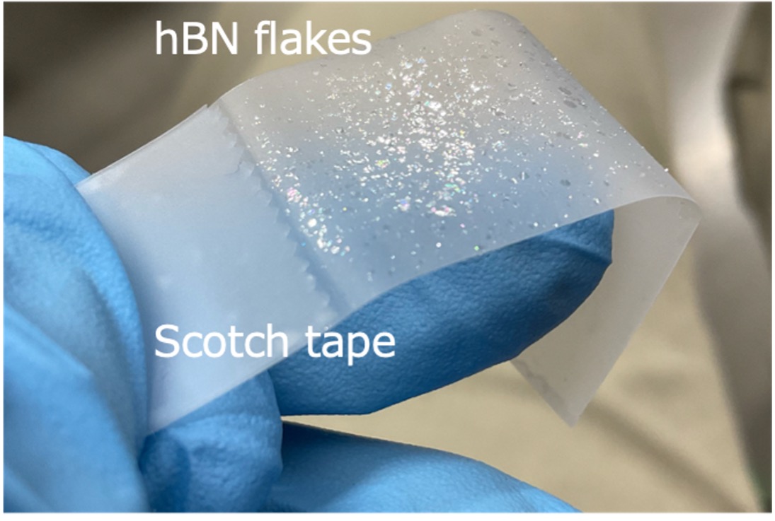
Hexagonal boron nitride flakes peeled by scotch tape. This allowed the researchers to create a thin layer to attach to a target gold wire.
The team obtained a thin hexagonal boron nitride film by pulling the Scotch tape off the crystal. The researchers attached the thin film to the target gold wire. Then they bombarded the film with a high-speed helium ion beam, thus popping boron atoms out and forming the boron vacancy spots of 100 nm2. Each spot contains many atom-sized vacancies which behave like tiny magnetic needles. The closer the spots are to each other, the better the spatial resolution of the sensors.
As current flowed through the wire, the team measured the magnetic field at each spot based on the intensity of light emitted from the spots in the presence of microwaves. The researchers were amazed when the measured values of the magnetic field matched closely with the simulated values, proving the efficacy of the high-resolution quantum sensors.
The change in the spin state of the sensor in the presence of a magnetic field can be detected even at room temperature, thus enabling easy detection of the local magnetic field and currents. Moreover, the boron nitride nanofilms attach to objects just by van der Waals force, which means the quantum sensors easily stick to different materials.
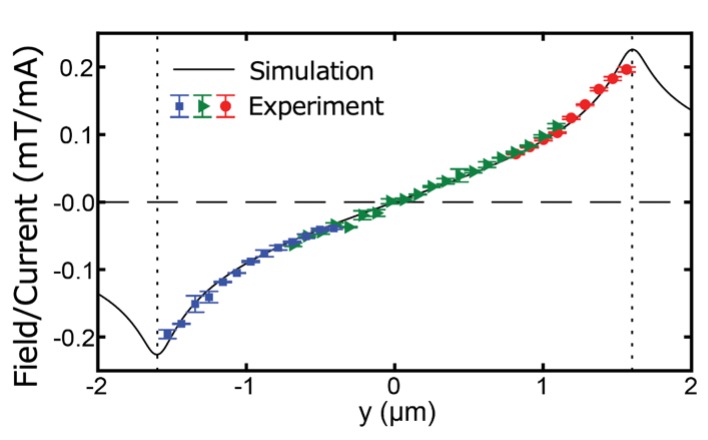
Imaging of the magnetic field created by the current flowing through a gold wire. This is the result of analyzing the magnetic field data for each spot. The excellent agreement of the experimental result with the simulation result proves the principle of the quantum sensor nanoarray.
Sasaki and his team plan to apply this technique for research on condensed matter physics and quantum materials. “It will enable direct detection of the magnetic field from, for example, peculiar states at edges of graphene and microscopic quantum dots,” adds Sasaki.
Atom-sized quantum sensors are starting to revolutionize how we sense microscopic environments and thus also understand macroscopic properties. Their applications run beyond basic science research. They can help image human brains, accurately geolocate, map underground environments, and detect tectonic shifts and volcanic eruptions. Sasaki and his team await the potential uses of their nanoscale quantum sensors in semiconductors, magnetic materials, and superconductors.
###
This research is a collaboration between the University of Tokyo, the National Institute for Materials Science (NIMS), and the National Institute of Advanced Industrial Science and Technology (AIST).
Publication details
Journal Applied Physics Letters Title Magnetic field imaging by hBN quantum sensor nanoarray AuthorsKento Sasaki, Yuki Nakamura, Hao Gu, Moeta Tsukamoto, Shu Nakaharai, Takuya Iwasaki, Kenji Watanabe, Takashi Taniguchi, Shinichi Ogawa, Yukinori Morita, and Kensuke KobayashiDOI